
200W Class-D Audio Power Amplifier [150115]
This is a single PCB 200 W Class-D Audio Power Amplifier fully designed with through hole components (external symmetrical power supply is needed).
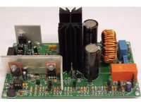
New Audio Power Amplifier (150115, PCB 150115-1 v2.1)
It’s been three years since we presented our Q-Watt amplifier (110656). It’s a standard Class AB amplifier with a lot of power and low distortion.. Here we present a fairly simple Class D amplifier, although at first glance the schematic may make one think otherwise. A large part of the schematic is for protection. However, the main amplifier part consists only of an integrated circuit (16-pin DIP) and a double power MOSFET (half-bridge package, 5-pin TO220). No other PCB is required, only a decent symmetrical power supply. We recommend the use of a stabilized power supply, specifically designed for Class-D amplifiers. All auxiliary power supply voltages (+5 V, -5 V and +12 V) are derived from the main power supply. All parts are through hole which makes changing and experimenting with the design easy.A possible option to design a Class D amplifier is an entire discrete solution, but that wouldn’t be a simple design. Many manufacturers have single chip solutions for class-D amplifiers. If you are looking for low power amplifiers these days there are countless ICs. If we look for high power and good quality there are not that many options. An excellent solution is an integrated circuit made by International Rectifier, the IRS2092. Titled ‘Protected Digital Audio Amplifier’ this 16-pin IC has all what it takes except for the power transistors. It’s a has a high current gate drive stage, Self-Oscillating PWM modulator, bidirectional over-current protection, programmable deadtime and can operate up to 800 kHz. In addition to the datasheet and numerous application notes International Rectifier also has quite a lot of reference designs with the IRS2092. Why invent the wheel again if somebody already did it for you. But as one might guess, our design is more than just an easy copy of a reference design.
In addition to the current protection of the IRS2092 we added some additional protection circuits: over-voltage protection (both supply voltages), under-voltage protection (both supply voltages) and a DC protection. Each of these protections, if triggered, disable the output relay and shut down the IRS2092. Usually if a power transistor fails it becomes a short circuit. In such case the load is safely decoupled form the amplifier by a relay.
Using a dedicated IC for any application usually means using the standard application from the manufacturer. In case of the IRS2092 this is not any different. A detailed description of the IRS2092 can be found in application note AN-1138 (IRS2092(S) Functional Description). Most external components needed have a fixed purpose. Most resistors connected to the IC define the two current limits, deadtime, bootstrapped drive voltage for the high side MOSFET and feedback of the output. The footprint for the capacitors that are part of the PWM modulator and RF decoupling of the audio input signal (C1/C5/C7/C8/C9) is designed so high quality radial polystyrene versions (lead spacing 7.07 mm diagonal), polypropylene versions or even standard polyester ones (lead spacing 5 mm) can be used. For a RF decoupling of the feedback (C6) a high quality 500 V 150 pF silver mica version is used. It has a very specific lead spacing (5.9 mm ) and it is strongly advised to use this capacitor and nothing else. For DC blocking capacitor (C4) at the input a standard MKT version is used. A polypropylene version would be preferable but the increase in size would mean more reception of noise and switching artifacts at the input stage, considering this type of amplifier.
Instead of deriving the +5 V (VAA) and -5 V (VSS) supply voltages, needed by the IRS2092, directly from the main power supply (e.g. just using resistors and maybe two additional Zener Diodes) we used 5 V regulators for optimum performance. In case the main supply is not regulated (not recommended), this is mandatory. An extra decoupling has been placed in series with VAA and VSS (R10/C10/C11 and R11/C12/C13) to prevent RF switching frequencies from influencing the two analog regulators. To limit the input voltages of the regulators to a safe level and prevent excessive power dissipation Zener Diodes (D4/D5) are placed at the inputs. The power supply can be as high as +/-70 V. Diode D3 protects the IRS2092 if a negative supply is missing. Without D3 VSS can go below COM.
The low side supply (VCC, pin 12) is referenced to the negative main power supply voltage. Since more power is taken from this regulator (IC5) an extra Darlington Power Transistor (T2) is used as a buffer for the input voltage of the +12 V regulator. This way the resistor needed to limit the voltage (R30) can have a relatively high value and no real power is lost here. The relation between level of the main power supply voltage and power dissipated by T2 is now linear. The VCC pin of IC2 is locally decoupled by C20 and R15.
VB is the floating high side supply for driving the high side MOSFET. This power supply is created by a standard bootstrap circuit consisting of R16/D6/C21 and R21 (necessary for charging C21 before PWM start up). R16 limits surge currents.
Deadtime can be programmed by voltage divider R19/R20: 105/65/40/25 ns. In our case deadtime can set to its minimum value of 25 ns by omitting R20. In this case R19 should be smaller than 10 kΩ. Relation VDT/deadtime: VCC/25 ns, 0.46*VCC/40 ns, 0.29*VCC/65 ns, COM/105 ns. 40 ns can be set by using a 4.7 kΩ resistor for R20. Increasing deadtime will increase THD at high frequencies considerably! Note that it takes a MOSFET generally about twice as long or more to turn off as to turn on. The gate resistors are R25 and R26 and limit the charge and discharge currents.
The voltage divider R17/R18 sets the low side over current threshold. RDS(on) of the output
MOSFETs is used as a current sensing resistor. An advantage is the positive temperature coefficient of RDS(on). The maximum current setting decreases with increasing temperature of the MOSFET. The IRS2092 has a reference voltage of 5.1 V (VREF, pin 7) for accurately setting the current threshold. However, the drain-source resistance of a MOSFET has a fairly large tolerance. At a gate-source voltage of 10 V the RDS(on) of the transistor used (IRFI4020H-117) is 80 mΩ typical and 100 mΩ maximum (TJ = 25°C). RDS(on) increases to more than 175 mΩ (typ.) at TJ = 125°C. We set the threshold voltage at 1.56 V, thus setting the current threshold at 19.5 A typically (TJ = 25°C). A junction temperature of 125°C reduces the current threshold to roughly 8.7 A. The pulsed drain current of the transistor used is 36 A, but is limited by the maximum junction temperature. If the output current is to high switching operation of the IRS2092 will shut down and outputs LO and HO will become low and protect the MOSFETS.
The high side current sensing takes a little more than just a voltage divider. An external reverse blocking diode (D7) is required to block high voltages from feeding into the CSH pin while the high side is off. Due to a forward voltage drop of 0.6V across D7, the measured drain-source voltage of the high side MOSFET is 0.6V higher. Pin CSH is the high side over current sensing input and it has fixed threshold of 1.2 V with respect to VS. R24 biases D7 when the high side MOSFET is switched on. Voltage divider R22/R23 reduces the voltage across the high side MOSFET and D7. So if we want to set the same current threshold as on the low side we have to take D7 into account:
R23 is 10 kΩ, VDS = 1.56 V (19.5 A * 80 mΩ), VD7 = 0.6 V
R22 = ((VDS + VD7 - 1.2) * R23)/1.2 = 8 kΩ (rounded to E-12 value 8.2 kΩ)
The short circuit currents of the gate driver outputs are 1 A for sourcing and 1.2 A for sinking. With 18 Ω for gate resistors R25 and R26 the peak charge/discharge currents are limited to about 0.5 A.
Capacitors C22-C28 are the necessary decoupling of the power supply. As with all Class-D amplifiers there is a problem called Bus Pumping. Energy from the output filter is flowing back to the power supply. This happens particularly at high levels, low frequencies and lower load impedances. In case a regulated power supply is used its feedback may become instable. The easiest way to suppress the rise in voltage of the power supply is to place large capacitors parallel. Start with two 10000 µF/100 V capacitors (one on each power supply line). But be careful, most switched mode power supplies have a problem with large capacitive loads. Look carefully at the SMPS’s specifications of the manufacturer what load the supply can handle and if this is necessary at all.
Additional protections:
As with all power amplifier there is always the chance something goes wrong. Hopefully that will never happen but in case one of the output transistors short circuits and one of the power supply voltages appears permanently at the output, it could damage the connected speaker system. To avoid this from ever happening a DC-protection is added. The level at which the DC-protection will act is set to a few volts. Reason for this is the DC appearing at the output of the amplifier when there’s no load and the IRS2092 is shut down. Apparently there is a residual current flowing from VS when the IRS2092 is in shut down mode. The DC-protection consists of R38/R39/R40/C34/T6/T7. Voltage divider R39/R40 makes the DC-detection less sensitive. With 4.7 kΩ for R40 the DC-protection levels are +3 V and -4 V. Without R40 the levels are +0.55 V/-1.85 V. If the DC-protection is more sensitive the output relay will never turn on because of the voltage drop across the feedback resistor. An extra zero load could reduce this offset but this would mean extra power loss. The levels set by R40 may be a little higher than customary, but shouldn’t prove harmful for any speaker system. If T6/T7 are becoming conducting enough T5 switches T4 on. T4 discharges C35 and the relay is deactivated. To activate the relay a small MOSFET T8 is used so capacitor C35 for the delayed turn-on of the relay can be kept small. This increases the speed in which C35 can be discharged in case one of the protections respond.
At the same time the IRS2092 is shut down by discharging C14 at pin CSD through T3.CSD is referenced to VSS (-5 V). T3 acts as a level shifter. D11 is added to avoid the circuit around T4 biasing T3 continuously through R35. To test the DC-protection jumper JP2 is added. For normal operation place JP2 in position Amp. Another value for R40 can be tested should for one reason or another the DC level of VS (pin 13 of IC2) be higher or lower (in case a lower value for feedback resistor R7 is used) than the DC-protection.
Digital Audio MOSFET IRFI4020H-117P has a limited power handling. Although rated for 200 V maximum drain-source voltage the continuous drain current is only 9.1 A (TC = 25°C). At a case temperature of 100°C its only 5.7 A continuously. For this reason an over-voltage protection is necessary (limit the power dissipation at higher power supply voltages). This amplifier is designed to handle a maximum supply voltage of +/-70 V. The over-voltage protection acts if the power supply is few volts above +/-70 V (+75.2/-76.0). Two Zener diodes D15 and D16 are the key components here. Depending on the series resistors R52 and R53 T12 starts conducting and like the DC-protection T5 is switched on and the relay is deactivated. Diode D17 is added so the positive detection works. Without D7 and an over-voltage on the positive supply the emitter of T12 is pulled high and T12 wouldn’t conduct.
The under-voltage detection is more complex and also responsible for deactivating the relay on time when the amplifier is turned off so no load noise is heard in the speakers when the amplifier is turned off. Instead of two Zener diodes two extra transistors are used. T10 and T11 both conduct if the power supply lines are high enough and keep T9 from conducting. If T9 switches on so will T5. The relay will deactivate and IC2 will shut down. D14 prevents T11 from conducting when T10 is fully switched on. In this case the collector of T10 is approximately -0.6 V and without D14 the emitter of T11 would also be at a potential of -0.6 V. T11 would stay turned on to a very low power supply level. The positive under-voltage would not work properly. The levels are set by voltage dividers R49/R50 for the positive power supply and R47/R46 for the negative power supply. Values of R49 and R47 also depend on de base current of T11 and de emitter current of T10 respectively. With the present values the relay will deactivate if the power supply is less than 40 V (+38 V/-41 V).
At the input there is an option to select buffer IC1 with jumper JP1 if the input impedance of 3.33 kΩ is considered too low. The AD8031ANZ is a fast rail-to-rail opamp. It’s power supply is directly taken from the two 5 V regulators. Of course a little degrading of the specifications is to be expected. Implementing additional gain is also possible by placing a resistor for R3. With just R4 the gain is 1. With R3 the gain is R4/R3 + 1.
The mechanical stuff: three heatsinks and the inductor:
Only a small heatsink is needed for IC3. No insulation is necessary since the metal tab of a 7805 regulator is connected to ground. A 1 mm aluminum plate with a surface of 30 x 30 mm is will do. Keep it two to three millimeters from the PCB. Mount the little heatsink in such way a screw in the mounting hole of the PCB next to the regulator is still accessible.
IC4, IC5 and T2 are mounted on the same 2 mm aluminum plate. Our plate is 27 x 90 mm. Keep it at least 5 mm from the PCB to avoid making contact with other components. All three have to be insulated! First determine the position of the two holes. We can give you a head start. The two holes are exactly 40 mm apart. The hole for IC4 is located 14 mm from the edge of the PCB. The height of the two holes you have to determine yourself, that shouldn’t be too difficult. But they should be about 12 mm from the bottom edge. After drilling the two holes make a 90° bend in the plate away from the heatsink for T1 at 65 mm. The photos show what it should look like.
The package of T1 is completely plastic and makes it easy to mount on the heatsink, no insulation is required. Just apply a very thin layer of thermal grease on the back of the package and use a 12 mm M3 screw, washer, locking ring and nut to securely mount the transistor. Before tightening the screw place the heatsink with the transistor on the PCB so the leads of the transistor fit through the appropriate holes without force. Now you can tighten the screw firmly and solder the heatsink. You should solder the five leads of T1 only when this is done.
The output inductor
Mounting and soldering the components is pretty straight forward and shouldn’t pose a problem. The only ‘difficult’ component is the inductor in the output filter. It has to be constructed by hand using a toroid of 33 mm (1.3 inch) in diameter and 1.5 mm enameled copper wire. The iron powder core used for the toroid is made of -2 material from Micrometals. Detailed information of the material can be found on their website. Just a small warning if you’re not used to it: Oersted and Gauss are used instead of A/m and T (Tesla). The materials permeability is virtually independent of the applied magnetizing force. It will take about 70 A to saturate the finished inductor (of course the copper wired used can’t handle this). This assures an output filter with extreme low distortion. Downside is the low permeability. This means a fairly large number of turns is necessary to get the desired induction. A bigger core could mean less copper losses but certainly more core losses. The T130-2 core is also a compromise as far as its physical size and the amount of copper wire needed are concerned. In this case 2 meter 1.5 mm copper wire is enough. This will produce an inductor with approximately 20 mΩ DC-resistance. 22 µH means 45 windings (AL is 11 nH/winding). 45 windings however will not fit in a single layer in the inside diameter of the toroid. To keep the parasitic capacitance small we chose the hard way to create the inductor. Instead of placing 33 windings in a first layer and 12 on a second and simply make the ending lead long enough to come out parallel to the starting lead we did it differently (see photo of the finished inductor). The second winding is placed on top of the first winding in the inside of the toroid. The second winding is placed next to the first winding on the outside of the toroid. The third winding is placed next to the first winding on the inside and next to the second winding on the outside. With the fourth winding this process starts over. When the 45 windings are completed the two leads of the inductor are on opposite sides of the toroid. Maybe you have to cheat here and there and it’s wise to keep track of the number of turns. The toroid is placed vertically on the PCB to save space. Although copper is a soft metal, bending the copper wire as close and straight as possible to the core can prove to be tough. 1.5 mm copper wire is not that flexible. It takes strong hands to do this. Don’t use metal tools. These will damage the insulation of the wire. If the wire is wound very close to the core it will take less than two meters of wire.
Alternatives for T1.
In our design we used the IRFI4020H-117P from International Rectifier (now part of Infineon Technologies AG). It’s part of a family of dual-MOSFETs (Digital Audio MOSFETs in Half-Bridge) specifically designed for Class-D power amplifiers: type (UDS max., ID continuous, RDS(ON))
IRFI4024H-117P (55 V, 11 A, 48 mΩ)
IRFI4020H-117P (200 V, 9.1 A, 80 mΩ)
IRFI4019H-117P (150 V, 8.7 A, 80 mΩ)
IRFI4212H-117P (100 V, 11 A, 58 mΩ)
The IRFI4020H-117P we used is typically designed for a 200-300 W amplifier with an 8 Ω load only. Be careful in selecting the proper transistor for your needs. With a symmetrical power supply of +/-70 V it’s best the UDS of the transistor used is at least 10 to 20 V higher than 140 V. Although two of the family have a lower RDS(ON) their maximum power supply is severely limited. With the present design the IRFI4024H-117P cannot be used because of the under-voltage setting of plus or minus 40 V. The MOSFET should at least withstand 100 V when the amplifier is run on a power supply of +/- 45 V. In this case the IRFI4212H-117P could be used to deliver about 200 W in a 4 Ω load.
Measurements:
If a lower supply voltage is used a lower value for the feedback resistor R7 can be used. At a power supply voltage of +/-70 V distortion will increase due to much feedback of the PWM component in the output signal. At +/-60 V R7 can be reduced to 100 kΩ.
To power the amplifier we used a switched mode power supply from Hypex, the SMPS400A400 which is specifically designed to be used with Class D amplifiers. The output voltage is fixed but depends on the mains voltage. At 230 VAC input, the output voltage is +/- 62 V. In our building the mains voltage is a bit lower, around 222 VAC. So the supply voltage for the power amplifier was +/-60 V when we performed the measurements. At higher mains voltages power output is of course slightly higher. The power supply has an input range of 180-264VAC and 90-132VAC (jumper). With +/-60 V the amplifier can handle loads from 6 to 8 Ω. Lower impedances will cause the current protection to activate at higher power levels and shutdown the amplifier temporarily . Higher impedances will cause the output filter to peak. The values for L1 and C29 are a compromise for loads from 4 to 8 Ω. At 20 kHz and an 8 Ω load the amplitude increases to 0.8 dB and a 4 Ω load will cause the amplitude to drop 1.2 dB. At 6 Ω the amplitude is almost flat (+0.25 dB). Without a load the output filter will peak at about 45 kHz and the amplitude can increase to much more than a factor of ten. R28 and C30 limit this somewhat.
Measurements 8 Ω version, power supply +/-60 V (Hypex SMPS400A400), B = 22 kHz
R7 = 100 kΩ
Input sensitivity 1.3 V (189 W/8 Ω, THD+N = 1 %)
1.25 V (174 W/8 Ω, THD+N = 0.1 %)
Input impedance 3.33 kΩ
Sine-wave power 174 W (8 Ω, THD+N = 0.1 %, 1 kHz)
189 W (8 Ω, THD+N = 1 %, 1 kHz)
224 W (6 Ω, THD+N = 0.1 %, 1 kHz)
246 W (6 Ω, THD+N = 1 %, 1 kHz)
Low cut-off frequency 5 Hz
Amplitude at 20 kHz -1.05 dB (4 Ω)
(referenced to 1 kHz) +0.27 dB (6 Ω)
+0.87 dB (8 Ω)
Slew rate 15 V/µs (8 Ω)
Rise time 4.4 µs (8 Ω)
Signal to noise ratio >77 dB (B = 22 Hz…22 kHz linear)
(Referred to 1 W/8 Ω) >80 dBA
Harmonic distortion plus noise 0.014 % (1 kHz, 1 W, 8 Ω, B = 22 kHz)
0.004 % (1 kHz, 50 W, 8 Ω, B = 22 kHz)
0.005 % (1 kHz, 50 W, 8 Ω, B = 80 kHz)
0.024 % (20 kHz, 50 W, 8 Ω, B = 80 kHz)
0.024 % (1 kHz, 1 W, 6 Ω, B = 22 kHz)
0.0046 % (1 kHz, 50 W, 6 Ω, B = 22 kHz)
0.0057 % (1 kHz, 50 W, 6 Ω, B = 80 kHz)
0.045 % (20 kHz, 50 W, 6 Ω, B = 80 kHz)
Intermodulation Distorsion 0.013 % (1 W, 8 Ω)
(50 Hz :7 kHz = 4 :1) 0.023 % (50 W, 8 Ω)
0.013 % (1 W, 6 Ω)
0.017 % (50 W, 6 Ω)
Dynamic IM Distorsion 0.037% (1 W, 8 Ω)
(3.15 kHz square wave + 0.009 % (50 W, 8 Ω)
15 kHz sine wave) 0.043 % (1 W, 6 Ω)
0.008 % (50 W, 6 Ω)
Damping factor 174 (1 kHz, 8 Ω)
DC protection +3 V/-4 V
DC output offset 0.3 mV (prototype!)
Delay output relay 6 s
Efficiency 8 Ω 93 % (THD+N = 0.1 %)
93 % (THD+N = 1 %)
6 Ω 94 % (THD+N = 0.1 %)
95 % (THD+N = 1 %)
We recorded some plots with our Audio Precision Analyzer.
Plot A (AMP_4_6_8ohm_50W.emf) shows amplitude as a function of frequency with a 4, 6 and 8 Ω load. The three amplitudes at 20 kHz show how the filter is a good compromise for the different impedances. From 10 to 20 kHz deviation is approximately +/-1 dB. At 8 Ω (cyan) the output filter clearly shows its resonance frequency. At 6 Ω (green) the amplitude is almost flat and at 4 Ω (blue) the cut-off frequency is lower.
Plot B (THD+N_1W_50W_22kHz_80kHz.emf) shows distortion plus noise at 1 W and 50 W with a 8 Ω load and bandwidths of 22 kHz and 80 kHz. Measurements with the higher bandwidth are usually left out in datasheets of Class D amplifiers. The amplifier still produces output signals above 22kHz so it only fair to show them as well, whether you can hear them or not. The red curve shows distortion plus noise at 50 W when measured with 22 kHz bandwidth. The blue curve shows distortion plus noise at 50 W when measured with 80 kHz bandwidth. The cyan curve shows distortion plus noise at 1 W when measured with 22 kHz bandwidth. The green curve shows distortion plus noise at 1 W when measured with 80 kHz bandwidth. Measurements are made with a ninth order elliptic 200 kHz low pass filter in front of the analyzer to filter out all residual artifacts of the PWM modulation.
Plot C (FFT_1W_8ohm.emf) shows a Fourier analysis of a 1 kHz signal at 1 W into an 8 Ω load. No harmonics are visible, well maybe a second harmonic in the noise. Total harmonic distortion plus noise measures up to 0.014 % and is just all noise. In this and the next FFT the switch frequency of the power supply is clearly visible at 90 kHz (according to the datasheet from Hypex this should lie between 80 and 120 kHz), but it’s at a level of -82 dB, so nothing to worry about.
Plot D (FFT_50W_8ohm.emf) shows a Fourier analysis of a 1 kHz signal at 50 W into an 8 Ω load. Now harmonics are visible. Total harmonic distortion plus noise measures up to 0.004 %. The power supply frequency is at 96 dB and of no consequence.
Plot E (THDvsLVL_8ohm.emf) shows distortion plus noise as a function of output power at 1 kHz with an 8 Ω load and a bandwidth of 22 kHz to get the best assessment. From 50 W onward distortion slowly rises. As stated in the beginning with a normal mains voltage this amplifier is solid 200 W amplifier.
4 Ω configuration:
To use 4 Ω loads a different transistor should be used and the power supply should be +/-46 V absolute maximum. Only a few components need to be changed. The current protection needs to be set at a higher level. This means changing R17, R18 and R22. The 48 V relay can be connected directly to the power supply (no series resistor is needed) and a simple wire can be used for R44. Also the feedback resistor can be lowered to 75 kΩ. The power transistor of choice is IRFI4212-117P. That’s all. To calculate the values for the current protection resistors we use the maximum current in a 3 Ω load, which is 15.33 A (theoretically, 46/3). The typical RDS(ON) of the IRFI4212-117P is 58 mΩ and maximal 72.5 mΩ. At TJ = 125°C this resistance is about 1.8 times higher, so 130.5 mΩ. The voltage drop across is 2 V. This level is used to calculate R17, R18 and R22. At full power in a 3 Ω load the current protection will still kick in after a few seconds since the heatsink can’t handle this power, even if the efficiency is above 90 %.
Measurements 4 Ω version, power supply +/-46 V (Laboratory Power Supply), B = 22 kHz
R7 = 75 kΩ, R17 = 6.2 kΩ, R18 = 3k9, R22 = 12 kΩ, R44 = 0 Ω (wire), T1 = IRFI4212-117P
Input sensitivity 1.4 V (126 W/8 Ω, THD+N = 1 %)
1.33 V (113 W/8 Ω, THD+N = 0.1 %)
1.39 V (243 W/4 Ω, THD+N = 1 %)
1.3 V (215 W/4 Ω, THD+N = 0.1 %)
Input impedance 3.33 kΩ
Sine-wave power 113 W (8 Ω, THD+N = 0.1 %, 1 kHz)
126 W (8 Ω, THD+N = 1 %, 1 kHz)
215 W (4 Ω, THD+N = 0.1 %, 1 kHz)
243 W (4 Ω, THD+N = 1 %, 1 kHz)
276 W (3 Ω, THD+N = 0.1 %, 1 kHz, a few seconds before shut down)
297 W (3 Ω, THD+N = 1 %, 1 kHz, a few seconds before shut down)
Low cut-off frequency 5 Hz
Amplitude at 20 kHz -1.17 dB (4 Ω)
(referenced to 1 kHz) +0.21 dB (6 Ω)
+0.87 dB (8 Ω)
Slew rate 11 V/µs (8 Ω)
Rise time 4.4 µs (8 Ω)
Signal to noise ratio >78 dB (B = 22 Hz…22 kHz linear)
(Referred to 1 W/8 Ω) >81.5 dBA
Harmonic distortion plus noise 0.012 % (1 kHz, 1 W, 8 Ω, B = 22 kHz)
0.005 % (1 kHz, 30 W, 8 Ω, B = 22 kHz)
0.006 % (1 kHz, 30 W, 8 Ω, B = 80 kHz)
0.036 % (20 kHz, 30 W, 8 Ω, B = 80 kHz)
0.021 % (1 kHz, 1 W, 4 Ω, B = 22 kHz)
0.012 % (1 kHz, 50 W, 4 Ω, B = 22 kHz)
0.013 % (1 kHz, 50 W, 4 Ω, B = 80 kHz)
0.11 % (20 kHz, 50 W, 4 Ω, B = 80 kHz)
Intermodulation Distorsion 0.018 % (1 W, 8 Ω)
(50 Hz :7 kHz = 4 :1) 0.017 % (30 W, 8 Ω)
0.031 % (1 W, 4 Ω)
0.057 % (50 W, 4 Ω)
Dynamic IM Distorsion 0.030 % (1 W, 8 Ω)
(3.15 kHz square wave + 0.011 % (50 W, 8 Ω)
15 kHz sine wave) 0.041 % (1 W, 4 Ω)
0.011 % (50 W, 4 Ω)
Damping factor 205 (1 kHz, 8 Ω)
99 (1 kHz, 4 Ω)
DC protection +3 V/-4 V
DC output offset -0.4 mV (prototype!)
Delay output relay 6 s
Efficiency 8 Ω 95 % (THD+N = 0.1 %)
97.5 % (THD+N = 1 %)
4 Ω 93.5 % (THD+N = 0.1 %)
94 % (THD+N = 1 %)
With this configuration we also recorded some plots for comparison
Plot F (AMP_4_6_8ohm_30W_v2_46V.emf) shows amplitude as a function of frequency with a 4, 6 and 8 Ω load. The differences compared to plot A are minimal.
Plot G (THD+N_1W_50W_4ohm_22kHz_80kHz_v2_46V.emf) shows distortion plus noise at 1 W and 50 W with a 4 Ω load and bandwidths of 22 kHz and 80 kHz. The cyan curve shows distortion plus noise at 50 W when measured with 22 kHz bandwidth. The blue curve shows distortion plus noise at 50 W when measured with 80 kHz bandwidth. The green curve shows distortion plus noise at 1 W when measured with 22 kHz bandwidth. The red curve shows distortion plus noise at 1 W when measured with 80 kHz bandwidth.
Plot H (THDvsLVL_4ohm_v2_46V.emf) shows distortion plus noise as a function of output power at 1 kHz with an 4 Ω load and a bandwidth of 22 kHz. From 10 W onward distortion rises very slowly but above 150 W faster. We can call this configuration a 240 W amplifier.
4 Ω configuration with even lower feedback resistor (R7 = 47 kΩ):
While testing our first prototype of the amplifier a strange effect was noticed. Originally the feedback resistor R7 was given a value of 47 kΩ. When using a power supply of +/-70 V with 47 kΩ a 5 V peak input signal is needed. This way the feedback was maximal. That’s why a rail-to-rail opamp was added to increase sensitivity if needed (IC1). Testing a new design never starts at the maximum supply voltage but at a much lower value like +/-40 V. Slowly increasing the power supply distortion suddenly increased dramatically when the supply voltage reached 56 V. Apparently the feedback injected to much of the PWM output signal into the IRS2092. At the highest supply voltage 120 kΩ seems to be the best compromise. At lower supply voltages the feedback resistor can be reduced proportionally. At voltages below 56 V the feedback resistor can be reduced even more. Still using a supply voltage of +/-46 V the feedback resistor is reduced again to 47 kΩ.
Measurements 4 Ω version, power supply +/-46 V (Laboratory Power Supply), B = 22 kHz
R7 = 47 kΩ, R17 = 6.2 kΩ, R18 = 3k9, R22 = 12 kΩ, R44 = 0 Ω (wire), T1 = IRFI4212-117P
Input sensitivity 2.26 V (130 W/8 Ω, THD+N = 1 %)
2.09 V (113 W/8 Ω, THD+N = 0.1 %)
2.21 V (246 W/4 Ω, THD+N = 1 %)
2.05 V (214 W/4 Ω, THD+N = 0.1 %)
Input impedance 3.33 kΩ
Sine-wave power 113 W (8 Ω, THD+N = 0.1 %, 1 kHz)
130 W (8 Ω, THD+N = 1 %, 1 kHz)
214 W (4 Ω, THD+N = 0.1 %, 1 kHz)
246 W (4 Ω, THD+N = 1 %, 1 kHz)
269 W (3 Ω, THD+N = 0.1 %, 1 kHz, seconds before shut down)
311 W (3 Ω, THD+N = 1 %, 1 kHz, seconds before shut down)
Low cut-off frequency 5 Hz
Amplitude at 20 kHz -1.18 dB (4 Ω)
(referenced to 1 kHz) +0.187 dB (6 Ω)
+0.86 dB (8 Ω)
Slew rate 11 V/µs (8 Ω)
Rise time 4.4 µs (8 Ω)
Signal to noise ratio 83 dB (B = 22 Hz…22 kHz linear)
(Referred to 1 W/8 Ω) 86 dBA
Harmonic distortion plus noise 0.006 % (1 kHz, 1 W, 8 Ω, B = 22 kHz)
0.0043 % (1 kHz, 30 W, 8 Ω, B = 22 kHz)
0.0047 % (1 kHz, 30 W, 8 Ω, B = 80 kHz)
0.039 % (20 kHz, 30 W, 8 Ω, B = 80 kHz)
0.009 % (1 kHz, 1 W, 4 Ω, B = 22 kHz)
0.009 % (1 kHz, 50 W, 4 Ω, B = 22 kHz)
0.010 % (1 kHz, 50 W, 4 Ω, B = 80 kHz)
0.120 % (20 kHz, 50 W, 4 Ω, B = 80 kHz)
Intermodulation Distorsion 0.013 % (1 W, 8 Ω)
(50 Hz :7 kHz = 4 :1) 0.023 % (30 W, 8 Ω)
0.023 % (1 W, 4 Ω)
0.042 % (50 W, 4 Ω)
Dynamic IM Distorsion 0.019 % (1 W, 8 Ω)
(3.15 kHz square wave + 0.010 % (50 W, 8 Ω)
15 kHz sine wave) 0.027 % (1 W, 4 Ω)
0.009 % (50 W, 4 Ω)
Damping factor 201 (1 kHz, 8 Ω)
97 (1 kHz, 4 Ω)
DC protection +3 V/-4 V
DC output offset -0.4 mV (prototype!)
Delay output relay 6 s
Efficiency 8 Ω 93.5 % (THD+N = 0.1 %)
95 % (THD+N = 1 %)
4 Ω 93 % (THD+N = 0.1 %)
95 % (THD+N = 1 %)
For comparison two more plots were recorded:
Plot I (THD+N_1W_50W_4ohm_22kHz_80kHz_v2_46V_47kohm.emf) shows distortion plus noise at 1 W and 50 W with a 4 Ω load and bandwidths of 22 kHz and 80 kHz. The cyan curve shows distortion plus noise at 50 W when measured with 22 kHz bandwidth. The blue curve shows distortion plus noise at 50 W when measured with 80 kHz bandwidth. The green curve shows distortion plus noise at 1 W when measured with 22 kHz bandwidth. The red curve shows distortion plus noise at 1 W when measured with 80 kHz bandwidth.
Plot J (THDvsLVL_4ohm_v2_46V_2_47kohm.emf) shows distortion plus noise as a function of output power at 1 kHz with an 4 Ω load and a bandwidth of 22 kHz. From 10 W onward distortion rises very slowly but above 100 W faster. When we compare this plot to plot H the distortion at lower output levels is a little better and benefits from the lower value for the feedback resistor R7. Down side is the lower input sensitivity but that shouldn’t be a problem for most preamplifiers and other signal sources. If a higher sensitivity is needed use buffer amplifier IC1 (place jumper JP1 in position B). Place a resistor for R3 to turn the default buffer configuration into an amplifier. Some examples: 2 kΩ for an amplification of two and 1 kΩ for an amplification of three.
Bill of Materials 150115-1 v2.1
Resistor
R1,R8 = 1 kΩ, 5%, 0.25W, 250V
R2,R23,R24,R30,R34,R36,R37,R46,R50,R54 = 10 kΩ, 5%, 0.25W, 250V
R3,R20 = not mounted
R4 = 2 kΩ, 1 %, 0.25W, 250V
R5 = 330 Ω, 5%, 0.25W, 250V
R6,R18 = 3 kΩ, 1 %, 0.25W, 250V
R7,R52 = 120 kΩ, 5%, 0.25W, 250V
R9 = 470 Ω, 5%, 0.25W, 250V
R10,R11,R15,R31 = 10 Ω, 5%, 0.25W, 250V
R12,R13 = 1.8 kΩ, 5 %, 2W, 350V
R14 = 2.2 kΩ, 5 %, 0.25W, 250V
R16 = 4.7 Ω, 5%, 0.25W, 250V
R17,R35 = 6.8 kΩ, 5%, 0.25W, 250V
R19 = 5.6 kΩ, 5%, 0.25W, 250V
R21 = 33 kΩ, 5%, 0.25W, 250V
R22 = 8.2 kΩ, 5 %, 0.25W, 250V
R25,R26 = 18 Ω, 5%, 0.25W, 250V
R27 = 1 Ω, 5 %, 1W, 350V
R28 = 10 Ω, 5 %, 1W, 350V
R29 = 2.2 kΩ, 5 %, 2W, 350V
R32,R40 = 4.7 kΩ, 5%, 0.25W, 250V
R33,R43 = 15 kΩ, 5%, 0.25W, 250V
R38,R39,R45,R48,R51 = 22 kΩ, 5%, 0.25W, 250V
R41 = 1 MΩ, 5%, 0.25W, 250V
R42 = 10 MΩ, 5%, 0.25W, 250V
R44 = 2.7 kΩ, 5 %, 0.25W, 250V
R47 = 150 kΩ, 5%, 0.25W, 250V
R49 = 820 kΩ, 5%, 0.25W, 250V
R53 = 47 kΩ, 5 %, 0.25W, 250V
P1 = 1 kΩ, 150mW, trimmer, top adjust
Capacitor
C1,C5,C7,C8,,C9 = 1 nF, 1 %, 63 V, lead spacing 7.18mm, polystyrene
(EXFS/HR 1000PF +/- 1%, LCR Components)
C2,C3,C11,C13,C16,C18,C31 = 100 nF, 10%, 50V, X7R, lead spacing 5.08mm
C4 = 10 µF, 10%, 63V, MKT, lead spacing 15mm
C6 = 150 pF, 5%, 500V, silvered mica, lead spacing 5.9mm
(CD15FD151JO3F, Cornell Dubilier)
C10,C12,C14,C20,C32 = 10 µF, 20%, 50V, lead spacing 2 mm, 5x11mm
C15 = 10 nF, 10%, 100V, X7R, lead spacing 5.08mm
C17,C19,C33 = 1 µF, 20%, 50 V, lead spacing 2 mm, 5x11mm
C21 = 22 µF, 20%, 50 V, lead spacing 2 mm, 5x11mm
C22,C24 = 100 nF, 10%, 250V, MKT, lead spacing 7.5mm, 4x10mm
(B32520C3104K000, TDK)
C23,C25 = 680 µF, 20%, 100V, lead spacing 7.5mm, 18x40mm, 28mΩ/2.57A
(100ZL680MEFC18X40, Rubycon)
C26 = 100 nF, 10%, 200V, X7R, lead spacing 5.08mm
(C330C104K2R5TA, Kemet)
C27,C28,C30 = 100 nF, 5%, 400V, lead spacing 15mm, polypropylene
(B32652A4104J000, TDK)
C29 = 470 nF, 5%, 400V, lead spacing 15mm, polypropylene
(B32652A4474J000, TDK)
C34 = 100 µF, 20%, 10V, bipolar, lead spacing 2.5/3.5mm, diam. 8mm max.
C35 = 2.2 µF, 50 V, 2 mm pitch, 5x11 mm
Inductor
L1 = 22 µH, T130-2 toroid (Micrometals), 20x40mm max.(2 m 1.5 mm enameled copper wire)
Semiconductor
D1,D2,D11,D13,D14,D17 = 1N4148, 100 V, 200 mA, 4 ns
D3,D8,D9 = 1N4007, 1000 V, 1 A
D4,D5,D10 = BZX85C18 SB00018/E1, zener 18V 1.3W
D15,D16 = BZX55C68-TR, zener 68V 0.5W 6% (alt. BZX79-C68, NXP)
D6 = MUR120G, 200V 1A
D7 = BAV21, 250V 250mA
D12 = LED, green, 3 mm
T1 = IRFI4020H-117P
T2 = TIP122G
T3,T4,T6,T7,T9,T10,T11,T12 = BC547C, 45 V, 100 mA, 625 mW, hfe=400
T5 = BC557C, -45 V, -100 mA, 625 mW, hfe=400
T8 = IRFD210PBF, 200V, 600mA, 1W, 1.5Ω
IC1 = AD8031ANZ
IC2 = IRS2092PBF
IC3 = MC7805CTG, 5 V, 1 A
IC4 = MC7905ACTG, -5 V, 1 A
IC5 = MC7812CTG, 12 V, 1 A
Other
K1,K2,K3,K4,K5 = Faston, through hole, lead spacing 5.08 mm, tab 6.35mm x 0.81mm
PC1,PC2,PC3,PC4,PC5,PC6 = Terminal pin, 1.3 mm dia.
JP1,JP2 = 3-way pinheader, vertical, pitch 2.54 mm
JP1,JP2 = Shunt jumper, 2.54 mm spacing
RE1 = Relay, PCB, SPCO, 16 A, 48 V/5.52 kΩ
(RT314048, TE Connectivity/Schrack)
HS1 = Heatsink PCB mounted, 2.6°C/W, spacing 2 pins 25.4mm
(530002B02500G, Aavid Thermalloy, LLC.)
Heatsink IC4/IC5/T2, 2mm aluminium plate, 27 x 90 mm
Heatsink IC3, 1 or 2 mm aluminium plate, 30 x 30 mm
T2,IC3,IC4,IC5 = Insulating kit, thermal pad TO-220 + bush TO-220
IC socket DIP-16
IC socket DIP-8
Misc.
PCB 150115-1 v2.1
To connect the Hypex SMPS400A400 power supply:
- 1 x JST VHR series 3.96mm pitch 5 way 1 row female straight PCB connector housing RS Components 820-1188 (Pack of 5)
- 1 x JST VHR series 3.96mm pitch 3 way 1 row female straight PCB connector housing RS Components 820-1175 (Pack of 5)
- 5 x JST cable assembly with a crimp and a crimp RS Components 820-1135 (Pack of 5)
- 3 x Faston connector, female, insulated 6.35 mm
Want to build a project?
Bring your design to life with the Elektor PCB Service, powered by Eurocircuits. Upload the project files and order professionally manufactured PCBs or assembled boards through a proven European production platform.
Supporting KiCad, Eagle, Gerber, and ODB++ formats, the service is suitable for everything from prototypes and validation builds to series production and volume manufacturing.
Made in Europe. Fast. Reliable. Professional.
Updates van de auteur