
IoT Micro Power Supply [130560]
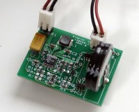
A small SMT PCB for a micro power supply for small indoor devices using a solar panel. With coin cell clip as an alternate power source.
Introduction:
The Internet of Things (IoT) defines a network of physical objects embedded with electronics, software, sensors and connectivity to provide services by exchanging data with the connected devices. It is an idea of globally interconnected continuum of devices, objects and things emerged with the RFID technology. It can also be considered as a scenario in which objects, animals or people are provided with unique identifiers and the ability to transfer data over a network without requiring human-to-human or human-to-computer interaction.
The goal of this project is to design a small SMT PCB for a micro power supply to power up small indoor devices using a solar panel and also including a coin cell clip as an alternate power source that can work with two different Buck-Boost converters namely LTC3129 and LTC3129-1. The board is so designed that both the IC’s can be used on the same PCB by using different component configuration. The major advantage of this project is that it can operate from an input source which is as low as 7.5uW so that a low cost small size solar panel can be used indoor.
The key features of LTC3129 and LTC3129-1 include a fixed 1.2MHz operating frequency, current mode control, internal loop compensation, automatic Burst Mode operation or low noise PWM mode, an accurate RUN pin threshold to allow the UVLO threshold to be programmed, a power good output and an MPPC (maximum power point control) function for optimizing power transfer when operating from photovoltaic cells.
Hardware:
K1 - Input source connector (Solar Panel sanyo – AM-1815) 4.9V.42uA
K2 - Output(Load) connector 3.0V - 3.2V
Bat1 – CR2032 type coil cell 3V.
Circuit description:
The circuit in exploits the unique ability of the LTC3129 and LTC3129‑1 to start up and operate from an input power source as weak as 7.5 microwatts—making them capable of operating from small, low cost solar cells with indoor light levels less than 200-lux.
To make the low current start-up possible, the LTC3129 and LTC3129-1 draw a meager two micro amps of current (less in shutdown) until three conditions are satisfied:
- The RUN pin must exceed 1.22V (typical).
- The VIN pin must exceed 1.9V (typical).
- VCC (which is internally generated from VIN but can also be supplied externally) must exceed 2.25V (typical).
Until all three of these conditions are satisfied, the part remains in a “soft-shutdown” or standby state, drawing just 2μA. This allows a weak input source tocharge the input storage capacitor untilthe voltage is high enough to satisfy allthree conditions,at which point the LTC3129/LTC3129-1begins switching, and VOUT rises to regulation,provided the input capacitor hassufficient stored energy.
The circuit is provided with a battery backup circuitry,a backup battery provides power when solar power is insufficient, where a primary lithium coin cell and a few external components have been added to provide backup power to the output. The LTC3129 is used in this case, allowing VOUT to be programmed for 3.2V to better match the voltage of the coin cell.
The input of the solar panel of 5V can be connected via connector K1 to expect an output of 3.2V on connector K2 of the example circuit. One can change the output voltage by configuring the feedback resistor values in the case of LTC3129 or by setting the 3 programmable pins in case of LTC 3129-1.provisions is made in the example circuit to maintain the stability of the output. The circuit can also operate without the coin cell battery.
Since the circuit is designed for indoor use an additional super charge capacitor is introduced in the circuit to store the day light. When the super charge capacitor is under charging circuit will not provide any rated output voltage until the super charge capacitor gets sufficient charge across it. Transistor T1 (FDC6312P) is used to switch between the convertor output and the battery output which is driven with the help of IC2 (74LVC2G04) which is an inverter driver by the PGOOD signal generated from the convertor IC when the input and output voltages are at rated value. If the input voltage is not sufficient then the PGOOD signal is not generated thus forcing the output voltage to switch onto the connected battery power.
Configurations and requirements for LTC3129 and LTC3129-1
RUN pin requirement
This pin is common in both IC’s and is an input to the RUN comparator the voltage on this pin should be above 1.1V to enable the Vcc regulator and above 1.28V to enable the converter. Connecting this pin to a resistor divider from VIN to ground allows programming a VIN start threshold higher than the 1.8V (typical) VIN UVLO threshold. In this case, the typical VIN turn-on threshold is determined by
VIN = 1.22V * [1+(R3/R1)]
As per our example circuit Since the input source current is of the order of uA ,hence a high value resistor is need to use, assuming R3 is selected as 4.22MOhm and VIN considered at 3.5V
3.5=1.22×[1+(4.22M/R1)]
Hence R1 = 2.26M
MPCP function
Maximum power point control programming pin (MPPC) is also common pin I n both IC’s. This pin connected to a resistor divider from VIN to ground to enable the MPPC functionality. If the VOUT load is greater than what the power source can provide, the MPPC will reduce the inductor current to regulate VIN to a voltage determined by:
VIN = 1.175V * [1 +(R4/R7)]
Assume R5 = 4.22MΩ
3.2=1.175×[1+(4.22M/R7)]
2.9787=[1+(4.22M/R7)]
R7=2.13MΩ ≈2.43MΩ
By setting the VIN regulation voltage appropriately, maximum power transfer from the limited source is assured. Note this pin is very noise sensitive; therefore minimize trace length and stray capacitance.
In our example the supply is less than 10mA and hence MPPC is not used in the example circuit and is connected to VCC through R10 which is 0 Ohm. The flexibility is provided on the board to use this function by configuring voltage divider values of resistors R4 and R7.
Feedback signal configuration for LTC3129
The feedback pin is a feedback Input to the Error Amplifier. This pin is connected to a resistor divider from VOUT to ground. The output voltage can be adjusted from 1.4V to 15.75V by:
Vout=1.175V*[1+(R1/R2)]
The feedback signal is adjusted by a voltage divider built around resistor R5 and R2 such that we get an output voltage of 3.2V from converter Vout=1.175×[1+(R5/R2)]
3.2=1.175×[1+(R5/R2)]
Assume R5 = 4.22MΩ
3.2=1.175×[1+(4.22M/R2)]
2.7234=[1+(4.22M/R2)]
R2=2.44MΩ ≈2.43MΩ
Output voltage Configurations in LTC3129-1
VS1, VS2 and VS3 are the output voltage select pins that need to be connected either to the ground pin or VCC for programming the output voltage. These pins should not float or go below ground. The configuration of these pins for the desired voltage is as follows:
Board using LTC3129
When a solar panel is connected to the input connector K1 whose voltage and current is 5V, 42uA, capacitor C7 starts to charge, since the charging current is too small, it takes 20-30 seconds to reach a voltage of 5V at the same time when the input supply voltage reaches 3.5V, the voltage on the RUN pin due to voltage divider built around R3 and R1 is equal to 1.28V which enables the converter output. At the same time the PGOOD signal is generated and sent to IC2 which controls the transistor T1 which in turn enables the output on connector K2 from converter IC1. The feedback from VOUT is sent to the feedback pin of IC1 via voltage divider built around R5 and R2 which determines the output voltage available at connector K2 which is set to 3 to 3.2V. The feed-forward capacitor C3 on the feedback divider is used to reduce burst mode Vout ripples.
If Bat1 is connected which is a 3V coin cell, In case of no solar panel or low light then the IC2 switches transistor T1 to connect to the battery power which is made available on connector K2.
When there is no PGOOD signal from the converter, the battery power can be used as an alternative source until there is no light or until the solar panel gets sufficient light.
If the super capacitor C10 is used when the solar panel is connected then the capacitor C10 starts to charge but due to the very low output current which is in microamps, C10 takes a long time to reach a rated output voltage of 3 to 3.2 V (8 – 12hrs). This enables to store the energy in the super capacitor and use it when required.
Board using LTC3129-1
Both the IC’s have the same functionality but the difference lies in their configuration in the circuit. LTC3129 uses a voltage divider on the feedback pin to set the output voltage while LTC3129-1 has VS1, VS2, VS3 pins that are used to set the output voltage.
The output is set at 3.3V using the configuration of VS1, VS2 and VS3 pins. The VC1 pin 7 of IC1 LTC3129-1 is connected to VCC pin through 0 Ohm resistor R8 and pin 2 that is VS2 is connected to the ground and Pin 5 which is VS3 is connected to ground through resistor R2 using 0 Ohm resistor.
MPPC pin is connected to VCC through 0 Ohm resistor R10 as this function requires input source more than 10mA. In case of other configuration and input source this function can be used and set by using voltage divider resistor R4 and R7. Other function of Battery and supercharge capacitor C10 are similar to LTC3129.
Building and Testing:-
The board can be built using any one of the chip either LTC3129or LTC3129-1 with their required components. Since maximum part is of SMD types and both IC’s have thermal pad and have to be soldered to PCB carefully to get good performance and stability on board. The board can be used with different possible configurations.
The components mark * are optional and need to be selected as per IC selection. The Feedback, RUN, and MPPC voltage divider resistor can be vary as per requirement and selection of input and output supply.
For LTC3129-1, the output can be configured up to 5V just changing the resistor configuration on VS1 and VS2 pins of IC1.
Connecting Battery and C10 super charge capacitor is depends on requirement whereas board can work without them.
To power the board, a solar panel of up to 5V supply can be connected as an input source at K1 and output can take out from connecter K2. By connecting Sanyo AM-1815 solar panel to connector K1, Board can be powered on at indoor light and if C10 super capacitor is used then it start changing as below...
As output of board is about 35 to 40uA at 3.2V. Let’s consider charging at 35uA and if it charges for 24 hours then it will give a charge of almost 700uAh equal to 7mA for 6 minutes which is almost 42mA for 1 minute.
Thus the power supply board is most suitable in applications where the power requirement of the devices is within above range.
Discussie (1 opmerking(en))