
Negative 150V power supply
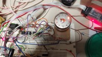
For a nixie-ish kind of project with ZM1050's I need a power supply of around 150V, 20mA. The twist is that is that the polarity must be negative with respect to common ground. And of course, I wanted to realize this with components laying around.
The Z550M or ZM1050 has been thoroughly described in the October 2009 issue of Elektor. Its datasheet proposes a power supply consisting of a mains transformer with 110V secondary, a rectifier and a small capacitor to eliminate voltage spikes. The rectified voltage needs to be negative with respect to the rest of the electronics, that can work on 5V. But, experimenting with a handful of these tubes, I found out that some of these old tubes just work better on a lower voltage. So I wanted to be able to regulate the voltage.
Also, for a good looking end result, I did not want to include a clumsy 110V mains transformer. There started the quest for a switching boost converter that can deliver negative 150V from positive 10 or 12V.
I had some old fashioned MC34063 IC's laying around, that I usually use for nixie-projects. The schematic for generating a hunderd or a couple of hundred volts is right in the datasheet and has also been published numerous times in Elektor. The resulting boost converter is not extremely efficient, but it does the job. The point is: all schematics that I found, in datasheets, application notes, Elektor, on the web, all generate a positive output voltage. I could have worked around that by including an isolating converter, then boost its output to 150V and connect the positive to ground, but mwha, switch converting the power twice? There must be a more direct way.
I thought I could modify the standard boost schematic with the MC34063 by using a P-MOSFET instead of the usual N-MOSFET. There is actually an example circuit in the datasheet of an inverter using a NPN-transistor. The problem with this circuit is that the negative output voltage is tied to the ground pin of the MC34063. Therefore this schematic is limited to about negative 40V, because otherwise the voltage differential between the input pin VCC and the ground pin goes over its absolute maximum rating of 50V.
In a first attempt, I removed all of the feedback and created schema2. This generates a voltage over -200V, so I knew I was on the right path. The P-channel MOSFET Q52 is switched rapidly on and off (at a frequency of about 40kHz) and each time Q52 is switched off, inductor L52 generates a rather high negative voltage, that is rectified by D52 and smoothed by C54.
This simple circuit has two disadvantages:
* there is no feedback, so the output valtage is more or less unpredictable and will vary heavily under load
* the MOSFET switch off is caused by the switch off of the internal transistor connected with its open collector on pin 1. The voltage on the gate of Q51 then rises to the input voltage because of R52. This causes the VGS of Q51 to become 0V and it switches off. This rise in voltage is unfortunately rather slow, because it's essentially an RC-circuit. In my experiments it took about 0.4µs. I'd like it to be an order of magnitude better.
FEEDBACK
I realized that repairing the feedback loop would require me to use some extra active component, because of the negative nature of the output voltage. So I decided to throw in an LM358 op-amp to invert the output voltage. First I was afraid that I would have to introduce a negative helper voltage fot the op-amp's negative power input, but fortunately I could avoid that. The LM358, although not a rail-to-rail op-amp, boosts "common-mode input voltage range includes ground, enabling direct sensing near ground", and that's exactly the feature that I need here. While the input on the left side of R53 may go below -150V, pin 2 of U52A will stay at 0V and the op-amp will output a positive voltage on pin 1. None of the op-amp pins will ever go negative. The feed-back Vfd pin 5 of U51 has a reference voltage of 1.25V, so by choosing R54 at 1250Ω, we know that the current through R54 and R53 will be 1mA and we can regulate the output voltage by choosing R53 as follows:
R53 Vout
50k 50V
100k 100V
150k 150V
BETTER SWITCHING
The standard way of improving the switch times of this circuit is by throwing in a BC547 and a 1N4148, so that is exactly what I did here. When the internal transistor in U51 goes on, the gate is charged through D51. When it goes off, the gate is discharged through the transistor. The current through R52 is only an fraction, so it will react much faster. In addition I took two other measures:
I included L51. You can consider this a AC decoupling of the node between U51, Q51 and D51. This makes switching faster. Another way to look at it: when the internal transistor switches off, there is still current going through L51 that wants to continue. Now this current cannot go through the internal transistor any more, it will try to find other ways and that will make the aforementioned node's voltage to rise rapidly. L51 doesn't need to be a power inductor. It can be a small axial inductor (internal resistance 2.5Ω).
I disconnected pin 1 of U51. Pin 1 is the output transistor of the MC34063, so it seems strange to disconnect this. I used pin 8 instead. Inside the MC34063 there are two transistors cascaded. In my experiments I found out that by omitting the final output transistor and using the intermediate transistor's output on pin 8, switching times improved. I can't fully explain this, but measurements proved it.
With these measurements in place, the rise time (switch off Q52) on the gate of Q52 went from 400ns to 46ns. The fall time (switch on Q52) went from 40ns to 110ns. The latter can be considered a deterioration, but on the other hand the current through Q52 is almost 0 at this point in time. The improvement in switch off is much more important, because at this time a substantial current is going through Q52, and the longer the switch off takes, the more Q52 heats up and energy is lost.
OTHER NOTES
The final schematic (KiCAD) includes two variants for switching the output on and off on the far right side. This is needed for the ZM1050. It requires a periodic shut off of the DC, otherwise, the display won't move from one digit to another. I haven't decided yet, but I think it's going to be the top variant with MPSA92 (PNP) and MPSA42 (NPN). Both variants are kind of a "high side switch", but on a negative power rail. The variant on the bottom uses a MOSFET. Normally, you would expect to see a P-channel MOSFET here, but as it is a negative voltage, we can just use an N-channel MOSFET. We still need to level-shift the control voltage from a logic level to the power level. In both variants, the MPSA92 takes care of this. MPSA's can handle up to 300V, so this is an easy task. In the final solution, of course I will connect R60 to the output of a microcontroller instead of the switch that is drawn here. Input high means disable output.
The output voltage can be regulated down on the fly by applying a small positive voltage on pin 3 of op-amp U42A. 0.625V on this pin will halve the output voltage. I think I may use an RC-filtered pwm output of the microcontroller for this purpose.
L52 is a radial power inductor 1.2A 0.45Ω or better.
FUTURE PLANS
I might consider ditching the MC34063 altogether and use the microncontroller for this task. The ATTINY 2313 that I'm planning to use has a built in comparator, voltage reference and PWM module, so the only thing I would still need is the LM358.
Want to build a project?
Bring your design to life with the Elektor PCB Service, powered by Eurocircuits. Upload the project files and order professionally manufactured PCBs or assembled boards through a proven European production platform.
Supporting KiCad, Eagle, Gerber, and ODB++ formats, the service is suitable for everything from prototypes and validation builds to series production and volume manufacturing.
Made in Europe. Fast. Reliable. Professional.
Discussie (0 opmerking(en))