
2nd version of Power bank for Laptop with batteries 18650: V3:
In the first version of this project, I was using some modules associated to an LM317 to charge the batteries. Here, it is new full schematic and more compact proposal, with more features such as display voltages and current, stop charge.
In the first version presented before, I was using some modules for the DC/DC boost (batteries to PC supply), DC/DC buck (charging batteries) and an LM317 for constant current.
This version has been used for months by my wife who has this PC with failed batteries. However, it is bulky proposal and suffer some small issues:
- Cannot switch off completely the device
- When connected to the PC power adaptor, the batteries 18650 are always under charge
- The display of voltage is power consuming and not user friendly
- No electrical information displayed or charge status.
The first target is to have a compact size. The PCB must fit with the bottom part of an holder for 2 batteries 18650.
This power bank will have 3 main functions now:
1) Convert the 2 batteries voltage to an 19V power supply for the laptop, with a max current of 3A
2) A recharge function for the batteries when the original PC power supply is connected (19v)
3) Display on an Oled screen the key parameters: Voltage to the PC, voltage from the battery, current from or to the batteries
Description first mock up:
1) On this part, still keep the LTC1871 as boost DC/DC (Vbat = 8.4V to V_PC = 19v). Made many calculation (based on datasheet) and tests with different frequency, inductor value.
2) For this first mockup, still use the LM2596 as Buck DC/DC (from V_PC 19v to Vbat charge = 8.4V max). After the LM2596, an LM317 mounted as current constant (400mA) limit the current to the batteries
3) Add a small MCU, PIC 12LF1840, with 2 I2C devices: An Oled display 0.91'' and an INA219 for current and battery voltage monitoring. A simple resistors divider monitor the PC voltage. The IN219 is associated to a small shunt 10mohm. At max output current, the batteries current is expecting to be more than 10A. so, the shunt must be as small as possible. A dedicated 3.3V regulator is implemented, capable to accept 20v as input
Result of the first mockup PCB:
- Beside the mistake made on the schematic, the routing of the PCB I made was not greatly done. The high current from the batteries to the DC/DC part had some grounding badly design
- It is not easy to find the right tradeoff for the inductor of the Boost DC/DC, the right frequency. At high output current (more than 1A), easy to heat and heater is mandatory on the switching mosfet and diode.
- The Buck DC/Dc to charge the battery works but the LM317 in constant current usage is easy to heat and not surface optimized
- The dedicated 3.3v for MCU/Oled display/INA219 has issue when high current supply to PC. Easy to get disconnected. Need to power the regulator from a diode and specific capacitor to protect against voltage drop
- The INA219 need very clean power supply. The routing of the ground was not optimized and create lot of wrong reading at high current output
- For the software (written in MikroC), had to struggle with the limited flash place (4KB). I2C function was rewritten to use less place. It is a simple loop to measure the PC voltage out (use ADC internal of the MCU), then read Vbus and Vshunt from the INA219. I do not use the internal capability of the INA for automatic calculation of power, current and so. Then display on the Oled if the value changed from previous loop. .For the Oled display, need use simple library. The original Oled library cannot fit in the 4KB place
New PCB for second mockup:
- Still keep the LTC1871 for the boost part. Cannot find better option yet
- For the buck DC/Dc and charging part, full redesign. Looking to use an MP1584, taking less place and use an operational amplifier to limit the current. Also, will implement a stop charge when the battery is full, either by software or hardware (hysteresis comparator)
Second PCB finalized (Oct 2023):
- Just finished on Oct 20th the second PCB
- Some changes compare to previous info:
* For the charging part, to make it more simple, use a dedicated Lithium circuit with buck embedded feature, LTC4002, which is available in 4.2 and 8.4v. It can accept from 5v to 22v input. Perfect for the usage here
* Add possibility to switch off and on the boost DC/DC with the uC
* Add a feature to be tested: When the formal PC power supply is plugged, switch of the boost converter. As soon as a small lower voltage is detected on this power supply (adjustable), the boost converter is power on. Need check if it can be fast enough to avoid power cut on V PC output
* Add another IN219 for measuring the current to the PC. By so, it can measure also the voltage and no need anymore the resistor divider and A/N function
* Add for the input DC power an micro USB plug. The idea is to have the possibility to use only one 18650 cell, charged with 5V USB and only be able to charge the PC (lower current)
* Rework the whole PCB to optimize the grounding, position of high current components
Second PCB testing results (Dec 2023):
After more than one month of testing, several improvements and corrections to be done:
* On the charging IC, LTC4002 8.4v, the Mosfet used was not correct. The VDS max was limited to 12v while it must be used with a normal PC charger which is more than 19v. So, another P Mosfet with higher VDS, other package now SO-8 is used. IRF9393 per example. We can see on the picture the small PCB with the mosfet on the inductor. Beside this, the LTC 4002 is working well. A sense resistor is used to fix the charging current: 100milliohm = 1A which is my configuration here
* The most tricky part was with the LTC 1871. Quite not easy to use. I redo several time the calculation for the inductor value, frequency, Mosfet Rdson, etc... The basics was Vin Min = 6v, Vout = 19v, Iout max 3A.
=> with all of this, got the I in Max current = 10A, I In peak = 12A. Inductor = 4.7uHand choose a Coilcraft with 14A Isat. I tried several frequencies and finally kept 220khz (120kohm)
=> On previous schematic, some mistake around the IntVcc of the LTC connected to the Vin. It was wrong as Vin will be more than 7V. They must be separated and IntVcc must be closely filter with a ceramic capacitor.
=> For the Mosfet, I choose an FDD8453 which claim to have Rdson 9milliohm
=> For the diode, use an SMB3045, 30A-45V
=> Add manually some ceramic capacitor 22uF 25v after the diode
The results is not as planned yet. Max current is 2A (3A is needed). After 2A charge, it looks like the security of the LTC1871 by sensing (via Sense pin) the current in the Mosfet is reducing the Vout. It is sure that the Mosfet FDD8453 is heating a lot and the Rdson increase. If the voltage on the sense pin is more than 100mv, it decrease the Vout. I need to try another Mosfet with even lower Rdson to check if the I out can increase.
* On the V2 schematic, I add a new feature. When the charger is connected, an NPN transistor (Q2) will disactivated the LTC for consumption saving (and by so increase the charging current in the batteries). With a finetune with the adjustable resistor (R22), it is working well. Below 18.5v the Dc/Dc is ON, above it is OFF. The test with high current load (2A) showed that the time when we remove the charger and the DC/Dc to start is less than 5ms drop to 18V.
* For the display and the software, the battery and output voltage are displayed. Also, the Input battery current (+ for charging and - for discharging) and the output current. However, the device is still fully functional without the PIC and display.
A new schematic and PCB is finished based on these corrections, V2.2 (Dec 1st 2023).
Test V2.2 (3rd Schematic and PCB version): (January 2024):
All the improvements works well here. Iout can be up to 3A (with IBAT > 10A).
However, some components need to be well choose.
The most important one is the MOSFET for the DC/Dc, Vbat to Vout. RDSon is critical.
Q1: IPD031N03L with RDSon 2.6mohm 30V 90A
Another RD3G600GNTL with 3.6mohm may be possible but not tested
D4 is SMB3045 (30A 45V)
L1 is an Colcraft 4.7uH. I choose the XAL1010-472MED with 24A saturation current
For the charging part, the mosfet (Q3) is here replace by a IRF9393 or Si4435.
On the PCBA, I used some tantale capacitors to save some place but some burnt... Maybe wrong quality. So, on the picture, they are replace by standard version.
I can now power my Asus with 3.1A. However, the batteries are heating quickly (more than 10A) and the L!/Q1 are heavily heating too. Some heaters are added.
Last improvements planned:
- 3D casing is under finalization. 3 versions already done...
- Schematic, V2.3 is slightly modified. I change the voltage adjustment resistor position in order to avoid high voltage if the resistor is at 0 (burnt tantale with that).
- Plan to add a fan in the casing to dissipate the heat. The fan will be power by the battery and start with an NTC
February 2024: Schematic V2.3:
Just uploaded what must be the last schematic. V2.3. Latest changes are:
- Due to the heat generated by the Dc/Dc (inductor and MosFET) and also by the batteries when battries current > 10A, I decided to add a fan in the casing. The fan is powered by a 5V IC linear DC/DC (IC3 LP2992 5v) in TSOP23. The ON/OFF pin is managed by 3 NPN 2N2222 (Q3/Q4?Q6). If the batteries voltage is below 5V, the fan need to stop to avoid deep discharge of the batteries. Then, an NTC (R2) checks the temperature (to be put either on the batteries or on the heater of the Mosfet / inductor). If the temperature is above 50 degres, the 5V IC is switch to ON.
- Adjust more precisely the RUN mode of the DC/DC U1. If VBAT is below 5.2v, the DC/Dc is OFF. Now, this create quite toogle mode as when the DC/Dc is stop, VBAT is increase a lot (much higher than the internal hysteresis of the RUN Pin) and the DC/DC restart.
- Change the voltage adjustment resistor R18 position to avoid high voltage is R18 is low value.
- Remove the USB plug feature. It was plan to have a version of this PCB with a single 18650 cell and work as standard power bank. I remove this possibility.
- Add a connection between Fan NTC and the uC to have possibility to display temperature...
November 2024: V3:
Despite the version V2.3 will be publish in Elektor, I continue to improve this version and made a V3 version with the following improvement:
- I found that in some case, using my Asus and charging it at max current (3.2A), when the AC/DC is power the PC through the power bank, there is not enough current to recharge the batteries (need 700mA). It looks like the external AC/DC switch off due to too much current requested. To avoid this, I connect one I/O from the uC to the COMP pin of the LTC4002-8.4. In that case, if the SW read that the PC is in charging more under external DC at more than 2.5A, it can disable the LTC4002 by putting low level to the COMP input.
- To recharge the batteries, before, only external AC/DC usage was possible. I made one USB charge cable with a boost DC/DC from 5v to 10v based on a module with MT3608. with a small heater on the MT3608, it can recharge overnight the batteries. In this new V3 version, I integrate the boost DC/DC with microUSB on the PCB (and remove useless screw connector for external power).
For the battery, I'll try to use RC lithium batteries (used for RC plane or car), 8.4v to see if it works longer that the 18650 (at least will have thinner casing)...
New PCB is launched to test this new version (and hope the last one)
Laurent
This version has been used for months by my wife who has this PC with failed batteries. However, it is bulky proposal and suffer some small issues:
- Cannot switch off completely the device
- When connected to the PC power adaptor, the batteries 18650 are always under charge
- The display of voltage is power consuming and not user friendly
- No electrical information displayed or charge status.
The first target is to have a compact size. The PCB must fit with the bottom part of an holder for 2 batteries 18650.
This power bank will have 3 main functions now:
1) Convert the 2 batteries voltage to an 19V power supply for the laptop, with a max current of 3A
2) A recharge function for the batteries when the original PC power supply is connected (19v)
3) Display on an Oled screen the key parameters: Voltage to the PC, voltage from the battery, current from or to the batteries
Description first mock up:
1) On this part, still keep the LTC1871 as boost DC/DC (Vbat = 8.4V to V_PC = 19v). Made many calculation (based on datasheet) and tests with different frequency, inductor value.
2) For this first mockup, still use the LM2596 as Buck DC/DC (from V_PC 19v to Vbat charge = 8.4V max). After the LM2596, an LM317 mounted as current constant (400mA) limit the current to the batteries
3) Add a small MCU, PIC 12LF1840, with 2 I2C devices: An Oled display 0.91'' and an INA219 for current and battery voltage monitoring. A simple resistors divider monitor the PC voltage. The IN219 is associated to a small shunt 10mohm. At max output current, the batteries current is expecting to be more than 10A. so, the shunt must be as small as possible. A dedicated 3.3V regulator is implemented, capable to accept 20v as input
Result of the first mockup PCB:
- Beside the mistake made on the schematic, the routing of the PCB I made was not greatly done. The high current from the batteries to the DC/DC part had some grounding badly design
- It is not easy to find the right tradeoff for the inductor of the Boost DC/DC, the right frequency. At high output current (more than 1A), easy to heat and heater is mandatory on the switching mosfet and diode.
- The Buck DC/Dc to charge the battery works but the LM317 in constant current usage is easy to heat and not surface optimized
- The dedicated 3.3v for MCU/Oled display/INA219 has issue when high current supply to PC. Easy to get disconnected. Need to power the regulator from a diode and specific capacitor to protect against voltage drop
- The INA219 need very clean power supply. The routing of the ground was not optimized and create lot of wrong reading at high current output
- For the software (written in MikroC), had to struggle with the limited flash place (4KB). I2C function was rewritten to use less place. It is a simple loop to measure the PC voltage out (use ADC internal of the MCU), then read Vbus and Vshunt from the INA219. I do not use the internal capability of the INA for automatic calculation of power, current and so. Then display on the Oled if the value changed from previous loop. .For the Oled display, need use simple library. The original Oled library cannot fit in the 4KB place
New PCB for second mockup:
- Still keep the LTC1871 for the boost part. Cannot find better option yet
- For the buck DC/Dc and charging part, full redesign. Looking to use an MP1584, taking less place and use an operational amplifier to limit the current. Also, will implement a stop charge when the battery is full, either by software or hardware (hysteresis comparator)
Second PCB finalized (Oct 2023):
- Just finished on Oct 20th the second PCB
- Some changes compare to previous info:
* For the charging part, to make it more simple, use a dedicated Lithium circuit with buck embedded feature, LTC4002, which is available in 4.2 and 8.4v. It can accept from 5v to 22v input. Perfect for the usage here
* Add possibility to switch off and on the boost DC/DC with the uC
* Add a feature to be tested: When the formal PC power supply is plugged, switch of the boost converter. As soon as a small lower voltage is detected on this power supply (adjustable), the boost converter is power on. Need check if it can be fast enough to avoid power cut on V PC output
* Add another IN219 for measuring the current to the PC. By so, it can measure also the voltage and no need anymore the resistor divider and A/N function
* Add for the input DC power an micro USB plug. The idea is to have the possibility to use only one 18650 cell, charged with 5V USB and only be able to charge the PC (lower current)
* Rework the whole PCB to optimize the grounding, position of high current components
Second PCB testing results (Dec 2023):
After more than one month of testing, several improvements and corrections to be done:
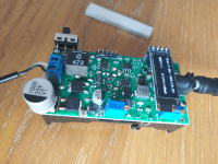
* On the charging IC, LTC4002 8.4v, the Mosfet used was not correct. The VDS max was limited to 12v while it must be used with a normal PC charger which is more than 19v. So, another P Mosfet with higher VDS, other package now SO-8 is used. IRF9393 per example. We can see on the picture the small PCB with the mosfet on the inductor. Beside this, the LTC 4002 is working well. A sense resistor is used to fix the charging current: 100milliohm = 1A which is my configuration here
* The most tricky part was with the LTC 1871. Quite not easy to use. I redo several time the calculation for the inductor value, frequency, Mosfet Rdson, etc... The basics was Vin Min = 6v, Vout = 19v, Iout max 3A.
=> with all of this, got the I in Max current = 10A, I In peak = 12A. Inductor = 4.7uHand choose a Coilcraft with 14A Isat. I tried several frequencies and finally kept 220khz (120kohm)
=> On previous schematic, some mistake around the IntVcc of the LTC connected to the Vin. It was wrong as Vin will be more than 7V. They must be separated and IntVcc must be closely filter with a ceramic capacitor.
=> For the Mosfet, I choose an FDD8453 which claim to have Rdson 9milliohm
=> For the diode, use an SMB3045, 30A-45V
=> Add manually some ceramic capacitor 22uF 25v after the diode
The results is not as planned yet. Max current is 2A (3A is needed). After 2A charge, it looks like the security of the LTC1871 by sensing (via Sense pin) the current in the Mosfet is reducing the Vout. It is sure that the Mosfet FDD8453 is heating a lot and the Rdson increase. If the voltage on the sense pin is more than 100mv, it decrease the Vout. I need to try another Mosfet with even lower Rdson to check if the I out can increase.
* On the V2 schematic, I add a new feature. When the charger is connected, an NPN transistor (Q2) will disactivated the LTC for consumption saving (and by so increase the charging current in the batteries). With a finetune with the adjustable resistor (R22), it is working well. Below 18.5v the Dc/Dc is ON, above it is OFF. The test with high current load (2A) showed that the time when we remove the charger and the DC/Dc to start is less than 5ms drop to 18V.
* For the display and the software, the battery and output voltage are displayed. Also, the Input battery current (+ for charging and - for discharging) and the output current. However, the device is still fully functional without the PIC and display.
A new schematic and PCB is finished based on these corrections, V2.2 (Dec 1st 2023).
Test V2.2 (3rd Schematic and PCB version): (January 2024):
All the improvements works well here. Iout can be up to 3A (with IBAT > 10A).
However, some components need to be well choose.
The most important one is the MOSFET for the DC/Dc, Vbat to Vout. RDSon is critical.
Q1: IPD031N03L with RDSon 2.6mohm 30V 90A
Another RD3G600GNTL with 3.6mohm may be possible but not tested
D4 is SMB3045 (30A 45V)
L1 is an Colcraft 4.7uH. I choose the XAL1010-472MED with 24A saturation current
For the charging part, the mosfet (Q3) is here replace by a IRF9393 or Si4435.
On the PCBA, I used some tantale capacitors to save some place but some burnt... Maybe wrong quality. So, on the picture, they are replace by standard version.
I can now power my Asus with 3.1A. However, the batteries are heating quickly (more than 10A) and the L!/Q1 are heavily heating too. Some heaters are added.
Last improvements planned:
- 3D casing is under finalization. 3 versions already done...
- Schematic, V2.3 is slightly modified. I change the voltage adjustment resistor position in order to avoid high voltage if the resistor is at 0 (burnt tantale with that).
- Plan to add a fan in the casing to dissipate the heat. The fan will be power by the battery and start with an NTC
February 2024: Schematic V2.3:
Just uploaded what must be the last schematic. V2.3. Latest changes are:
- Due to the heat generated by the Dc/Dc (inductor and MosFET) and also by the batteries when battries current > 10A, I decided to add a fan in the casing. The fan is powered by a 5V IC linear DC/DC (IC3 LP2992 5v) in TSOP23. The ON/OFF pin is managed by 3 NPN 2N2222 (Q3/Q4?Q6). If the batteries voltage is below 5V, the fan need to stop to avoid deep discharge of the batteries. Then, an NTC (R2) checks the temperature (to be put either on the batteries or on the heater of the Mosfet / inductor). If the temperature is above 50 degres, the 5V IC is switch to ON.
- Adjust more precisely the RUN mode of the DC/DC U1. If VBAT is below 5.2v, the DC/Dc is OFF. Now, this create quite toogle mode as when the DC/Dc is stop, VBAT is increase a lot (much higher than the internal hysteresis of the RUN Pin) and the DC/DC restart.
- Change the voltage adjustment resistor R18 position to avoid high voltage is R18 is low value.
- Remove the USB plug feature. It was plan to have a version of this PCB with a single 18650 cell and work as standard power bank. I remove this possibility.
- Add a connection between Fan NTC and the uC to have possibility to display temperature...
November 2024: V3:
Despite the version V2.3 will be publish in Elektor, I continue to improve this version and made a V3 version with the following improvement:
- I found that in some case, using my Asus and charging it at max current (3.2A), when the AC/DC is power the PC through the power bank, there is not enough current to recharge the batteries (need 700mA). It looks like the external AC/DC switch off due to too much current requested. To avoid this, I connect one I/O from the uC to the COMP pin of the LTC4002-8.4. In that case, if the SW read that the PC is in charging more under external DC at more than 2.5A, it can disable the LTC4002 by putting low level to the COMP input.
- To recharge the batteries, before, only external AC/DC usage was possible. I made one USB charge cable with a boost DC/DC from 5v to 10v based on a module with MT3608. with a small heater on the MT3608, it can recharge overnight the batteries. In this new V3 version, I integrate the boost DC/DC with microUSB on the PCB (and remove useless screw connector for external power).
For the battery, I'll try to use RC lithium batteries (used for RC plane or car), 8.4v to see if it works longer that the 18650 (at least will have thinner casing)...
New PCB is launched to test this new version (and hope the last one)
Laurent
Updates van de auteur