
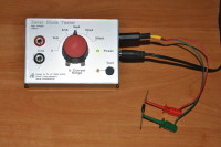
Zener Diode Tester
In this page I present my approach to building a Zener diode tester. There are of course several DIY versions on the internet, but I have a few requirements... I am often confronted with switching power supplies in which Zener diodes are used to stabilize certain voltages and the worst part is that too often their marking is illegible or almost non-existent. That's the whole point of this instrument.
In this article I present my approach to building a Zener diode tester.
There are of course several DIY versions on the internet, but I have a few requirements...
I am often confronted with switching power supplies in which Zener diodes are used to stabilize certain voltages and the worst part is that too often their marking is illegible or almost non-existent. That's the whole point of this instrument.
Most of the assemblies that I have seen on the Internet do not allow testing Zener diodes having a reverse voltage threshold greater than 30V. However, I have already been confronted with 33V or even 36V Zener diodes. To check these latest models it is therefore necessary to be able to exceed this threshold of 30V.
In an article published in the Elektor magazine in March 2010, such a device is presented, even making it possible to test diodes up to 200V, but it mainly uses two transformers (three if we consider the one reserved for the polarization of the small integrated panel voltmeter...). I have never been confronted with such high values which do not interest me in this project, and on the other hand I did not want to exceed the 48V threshold for simple safety reasons. The use in the previously cited article of a current source does not leave me indifferent, and I took inspiration from it here.
However, I draw your attention to the fact that this instrument is not intended to control a Zener diode on a circuit; it must be removed before any measurement.
My requirements and/or constraints
The oscillator and its chopper circuit
As soon as the power is turned on via the 12V socket (I have not provided a general switch...) the oscillator organized around the NE555 starts at a frequency of approximately 1.4 KHz, the chopper circuit made up of transistor T1 (IRF740 - MOSFET Channel N) and inductance L1 (4.7 mH) only starting to cut out when the push button is pressed. The advantage of this functionality is to avoid overheating in the inductor as much as possible. The operating frequency was chosen following several manipulations with my function generator in order to obtain a voltage greater than +40V on the cathode of the Schottky diode D1 (SB120). Resistor R6 (47 kΩ) is used to discharge the filter capacitor C3 (1 µF/100V).
The push button only powers the chopper circuit when it is pressed, the oscillator circuit remaining continuously powered. The reason is that in view of the oscillogram the potential difference of 1VC/C present on resistor R5 (1 Ω) implies a current of 1A (we are in the presence of an impulse regime here. ..) for a maximum power of 1W. The trace CH I corresponds to the signal recorded on the drain of the transistor, while the trace CH II is that of its source in relation to ground, and therefore of the signal absorbed by resistor R5. The progressive rise corresponds to the accumulation of energy in the inductance during conduction (ton=294 µs) of the MOSFET transistor.
The inductor I selected comes from an old power supply. switching and I do not know its characteristics apart from its value indicated on the body (small problem during my manipulations, I had to repair it, a broken pin is the reason for this yellow sheath...). It reaches more than 40°C quite quickly, which actually suggests that it is not capable of working for a long time under this high current. We should probably prefer an inductor like the Murata 1447509C model for example, but the dimensions of my PCB do not allow it to be placed there, so we would have to review everything... :-(
However, the measurement time being relatively short, a few seconds at most, this remains acceptable for sporadic use.
Another approach would be to use an inductor of 15 µH for example, and modify the oscillator circuit to reach a frequency of around 50 KHz... why not... the one I have in stock did not accept operate in such a system...
The constant current source
A constant current source maintains a predefined current (here depending on the resistors R9 to R13) through a load composed of the Zener to be tested (D.U.T) in series with the diode D2 which only serves as protection against short circuits, whatever its value. Thus if we consider the base current of T2 as negligible compared to its emitter current, we can estimate that the collector current is almost equal to the current circulating in the emitter junction.
This current source is composed of transistor T2 (BD140) in 'common base' mode, Zener diode ZD1 (BZX55C 4.7V) and resistor R8 (2.2 kΩ) polarizing its base. A rotary switch allows you to select a resistance from the 5 available in order to choose a current for the measuring circuit. The values of these resistors have been calculated in order to obtain the proposed currents, namely 1 mA / 2 mA / 5 mA / 10 mA and 50 mA. The method for calculating these values is simply as follows:
I = (VZD1 - VBE) / Emitter resistance which gives us with the standard values of the E24 series:
I = (VZD1 - VBE) / R9 = (4.7V - 0.6V) / 3900 Ω = 1.05 mA
I = (VZD1 - VBE) / R10 = (4.7V - 0.6V) / 2000 Ω = 2.05 mA
I = (VZD1 - VBE) / R11 = (4.7V - 0.6V) / 820 Ω = 5.00 mA
I = (VZD1 - VBE) / R12 = (4.7V - 0.6V) / 390 Ω = 10.51 mA
I = (VZD1 - VBE) / R13 = (4.7V - 0.6V) / 82 Ω = 50.00 mA
To check the correct operation of this current source, it is possible to place for example a 100 Ω / 1% resistor in place of a Zener to be tested, measuring its potential difference must confirm the accuracy of the currents indicated above.
The total consumption of the instrument during a measurement is 165 mA at DC12V.
Realization
For this achievement I did not make a printed circuit but used two 60 x 40 mm plated boards mounted imperially. The first houses the oscillator and chopper circuits, the second the current source and its rotary switch.
However, I designed the single-board printed circuit in 95 x 65 mm format using Eagle v7.7.0, the Gerber files are included in my project archive. Maybe my personal copy will remain in prototype form, or not...
A keen eye will no doubt have noticed a small 'bizarre' printed circuit mounted on the lower board... this is a small SOIC-8 to DIP-8 adapter board as my NE555 is in CMS version. The component wrapped in yellow heat shrink tubing is the 4.7 mH inductor. As a push button, I used a model from the 'D6' series soldered to a small piece of hole test plates and fixed by means of the retaining screw of the two plates mounted imperially. The advantage of this arrangement is that the cap of the push button comes close to the box. That's a lot of parts added to each other but once again this is only a prototype.
You will also notice that the two transistors do not have coolers, although present in the diagram. I have only planned their locations on the final printed circuit, it will always be possible to add them if the need arises.
A small particularity concerning the value of 35.5 kΩ of resistor R3... this value does not exist even in the E96 series, the simplest is to use two resistors of 25.5 kΩ / 1% (E96 series ) and 10 kΩ / 1% (E24 series) connected in series thus becoming R3 and R3' respectively, which is what I did on my exemplary.
Finition
To design the front panel I used the excellent free software 'Front Panel Express' as usual. Laser printing carried out on a matte silver 'aluminium' style polyester adhesive support allows you to obtain a beautiful screen print. Despite everything, bubbles remain visible; this requires a very well prepared support.
This project is available on my personal website at this address: https://www.pleguen.fr
There are of course several DIY versions on the internet, but I have a few requirements...
I am often confronted with switching power supplies in which Zener diodes are used to stabilize certain voltages and the worst part is that too often their marking is illegible or almost non-existent. That's the whole point of this instrument.
Most of the assemblies that I have seen on the Internet do not allow testing Zener diodes having a reverse voltage threshold greater than 30V. However, I have already been confronted with 33V or even 36V Zener diodes. To check these latest models it is therefore necessary to be able to exceed this threshold of 30V.
In an article published in the Elektor magazine in March 2010, such a device is presented, even making it possible to test diodes up to 200V, but it mainly uses two transformers (three if we consider the one reserved for the polarization of the small integrated panel voltmeter...). I have never been confronted with such high values which do not interest me in this project, and on the other hand I did not want to exceed the 48V threshold for simple safety reasons. The use in the previously cited article of a current source does not leave me indifferent, and I took inspiration from it here.
However, I draw your attention to the fact that this instrument is not intended to control a Zener diode on a circuit; it must be removed before any measurement.
My requirements and/or constraints
- use as many recovery components as possible, mainly the inductance L1 (model retained of 4.7 mH)
- no transformer, power supply is provided by a small power supply. switching DC12V / 1A
- use of an existing box (sorry, no ref because it's an old model around 30 years old...) in my drawers, aluminium model, dimensions (L x W x H): 100 x 70 x 40 mm
- use the principle of a current source offering several measurement calibers
- do not exceed the threshold of 48V, voltage available on the two banana sockets in the absence of a diode to test (unless the switch is in the '0' position...)But how can I generate the potential difference necessary for the measurement without using a transformer, and all with a maximum of components (
The oscillator and its chopper circuit
As soon as the power is turned on via the 12V socket (I have not provided a general switch...) the oscillator organized around the NE555 starts at a frequency of approximately 1.4 KHz, the chopper circuit made up of transistor T1 (IRF740 - MOSFET Channel N) and inductance L1 (4.7 mH) only starting to cut out when the push button is pressed. The advantage of this functionality is to avoid overheating in the inductor as much as possible. The operating frequency was chosen following several manipulations with my function generator in order to obtain a voltage greater than +40V on the cathode of the Schottky diode D1 (SB120). Resistor R6 (47 kΩ) is used to discharge the filter capacitor C3 (1 µF/100V).
The push button only powers the chopper circuit when it is pressed, the oscillator circuit remaining continuously powered. The reason is that in view of the oscillogram the potential difference of 1VC/C present on resistor R5 (1 Ω) implies a current of 1A (we are in the presence of an impulse regime here. ..) for a maximum power of 1W. The trace CH I corresponds to the signal recorded on the drain of the transistor, while the trace CH II is that of its source in relation to ground, and therefore of the signal absorbed by resistor R5. The progressive rise corresponds to the accumulation of energy in the inductance during conduction (ton=294 µs) of the MOSFET transistor.
The inductor I selected comes from an old power supply. switching and I do not know its characteristics apart from its value indicated on the body (small problem during my manipulations, I had to repair it, a broken pin is the reason for this yellow sheath...). It reaches more than 40°C quite quickly, which actually suggests that it is not capable of working for a long time under this high current. We should probably prefer an inductor like the Murata 1447509C model for example, but the dimensions of my PCB do not allow it to be placed there, so we would have to review everything... :-(
However, the measurement time being relatively short, a few seconds at most, this remains acceptable for sporadic use.
Another approach would be to use an inductor of 15 µH for example, and modify the oscillator circuit to reach a frequency of around 50 KHz... why not... the one I have in stock did not accept operate in such a system...
The constant current source
A constant current source maintains a predefined current (here depending on the resistors R9 to R13) through a load composed of the Zener to be tested (D.U.T) in series with the diode D2 which only serves as protection against short circuits, whatever its value. Thus if we consider the base current of T2 as negligible compared to its emitter current, we can estimate that the collector current is almost equal to the current circulating in the emitter junction.
This current source is composed of transistor T2 (BD140) in 'common base' mode, Zener diode ZD1 (BZX55C 4.7V) and resistor R8 (2.2 kΩ) polarizing its base. A rotary switch allows you to select a resistance from the 5 available in order to choose a current for the measuring circuit. The values of these resistors have been calculated in order to obtain the proposed currents, namely 1 mA / 2 mA / 5 mA / 10 mA and 50 mA. The method for calculating these values is simply as follows:
I = (VZD1 - VBE) / Emitter resistance which gives us with the standard values of the E24 series:
I = (VZD1 - VBE) / R9 = (4.7V - 0.6V) / 3900 Ω = 1.05 mA
I = (VZD1 - VBE) / R10 = (4.7V - 0.6V) / 2000 Ω = 2.05 mA
I = (VZD1 - VBE) / R11 = (4.7V - 0.6V) / 820 Ω = 5.00 mA
I = (VZD1 - VBE) / R12 = (4.7V - 0.6V) / 390 Ω = 10.51 mA
I = (VZD1 - VBE) / R13 = (4.7V - 0.6V) / 82 Ω = 50.00 mA
To check the correct operation of this current source, it is possible to place for example a 100 Ω / 1% resistor in place of a Zener to be tested, measuring its potential difference must confirm the accuracy of the currents indicated above.
The total consumption of the instrument during a measurement is 165 mA at DC12V.
Realization
For this achievement I did not make a printed circuit but used two 60 x 40 mm plated boards mounted imperially. The first houses the oscillator and chopper circuits, the second the current source and its rotary switch.
However, I designed the single-board printed circuit in 95 x 65 mm format using Eagle v7.7.0, the Gerber files are included in my project archive. Maybe my personal copy will remain in prototype form, or not...
A keen eye will no doubt have noticed a small 'bizarre' printed circuit mounted on the lower board... this is a small SOIC-8 to DIP-8 adapter board as my NE555 is in CMS version. The component wrapped in yellow heat shrink tubing is the 4.7 mH inductor. As a push button, I used a model from the 'D6' series soldered to a small piece of hole test plates and fixed by means of the retaining screw of the two plates mounted imperially. The advantage of this arrangement is that the cap of the push button comes close to the box. That's a lot of parts added to each other but once again this is only a prototype.
You will also notice that the two transistors do not have coolers, although present in the diagram. I have only planned their locations on the final printed circuit, it will always be possible to add them if the need arises.
A small particularity concerning the value of 35.5 kΩ of resistor R3... this value does not exist even in the E96 series, the simplest is to use two resistors of 25.5 kΩ / 1% (E96 series ) and 10 kΩ / 1% (E24 series) connected in series thus becoming R3 and R3' respectively, which is what I did on my exemplary.
Finition
To design the front panel I used the excellent free software 'Front Panel Express' as usual. Laser printing carried out on a matte silver 'aluminium' style polyester adhesive support allows you to obtain a beautiful screen print. Despite everything, bubbles remain visible; this requires a very well prepared support.
This project is available on my personal website at this address: https://www.pleguen.fr
Updates van de auteur